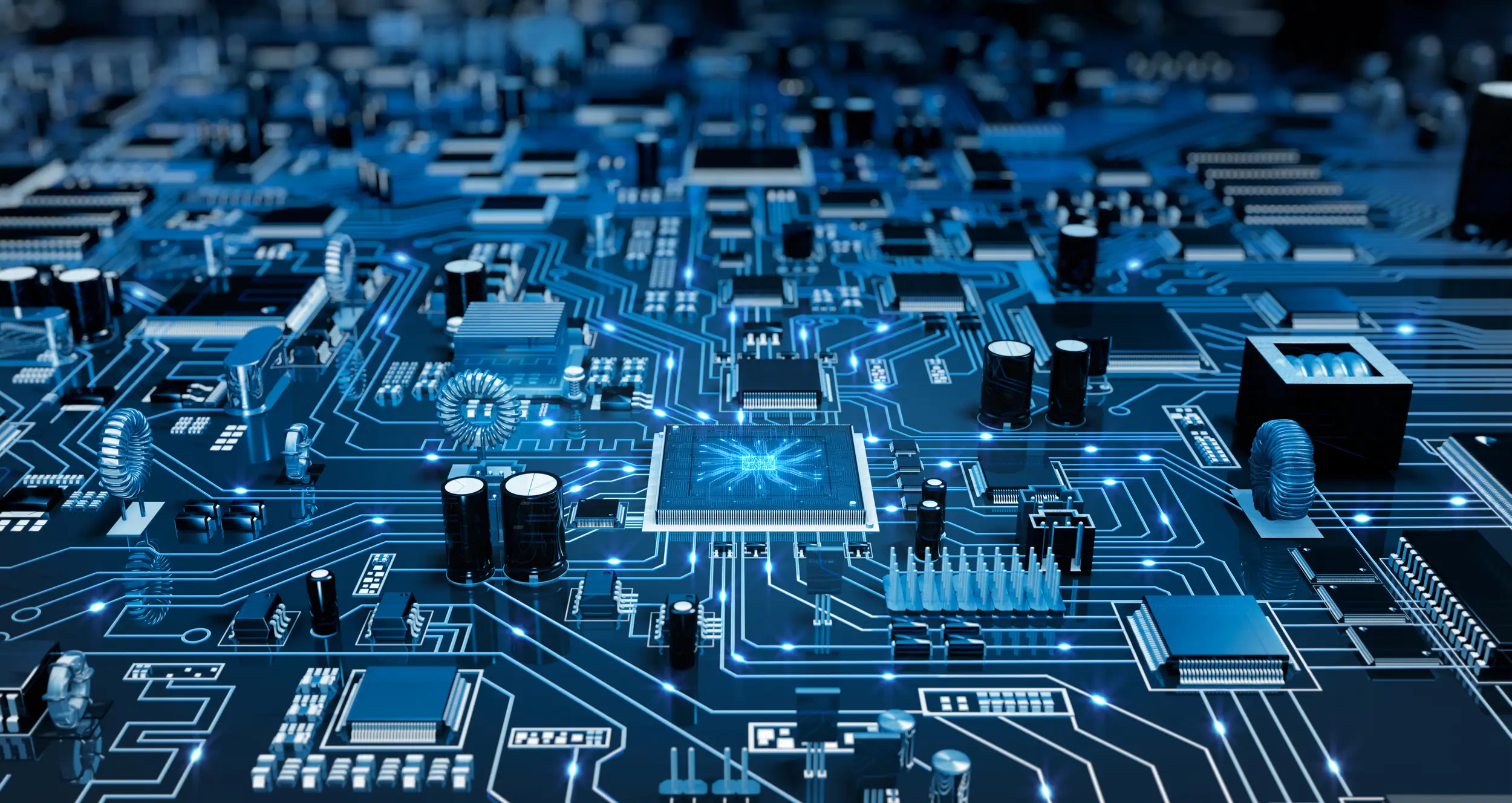
After all the components have been soldered and mounted on a printed circuit board, the finished board is referred to as a printed circuit board assembly (PCBA). PCBAs manufacturers require a number of steps including pcb design and prototype development.
When a PCB is finished, Active and Passive Electronic Components must be soldered onto it before it can be utilized in any electronic device or gadget. PCBAs manufacturers use conductive paths carved in the laminated copper sheets of PCBs to build the assembly within a non-conductive substrate. Attaching the electronic components to the PCBs completes the process of making an electronic device that works as intended.
Table of Contents
How PCB Assembly Works
A circuit board prior to assembly of electronic components is well-known as PCB. Printed circuit board assembly, also called PCB board assembly (PCBA), is the process of putting solder paste on the PCB or printed circuit board and putting together different parts like integrated circuits, resistors, and capacitors.
Stepwise Process of PCB board assembly
The assembling of a PCB is a straightforward procedure that includes both automated and human phases. PCBA manufacturers have both manual and automated choices for every stage of the process. Below, we explain each step of the PCBA process so you can see how it works from start to finish.
1. Solder the circuit board using paste
Using a mechanical device, apply the stainless steel stencil made of thin material across the board. On the circuit board, solder paste should be evenly spread in the required places by PCBAs manufacturers.
2. Select and position the device
A robotic device should be working on attaching SMDs or surface mount components to a prepared PCB. Following that, the parts must be soldered to the circuit board’s surface by PCBAs manufacturers.
3. Allow the solder paste to set
The solder paste needs to reflow and stay in place for a long time in order to bond the components to the PCB.
4. Look over the PCB assembly
The PCB inspection happens after the reflow procedure goes to the final step and the mount components are patch-up into place. There needs to be thorough examination and testing of the new PCB board. There are several ways to check the PCBA for quality control.
4a. Manual checks
An in-person visual examination performed by a designer to guarantee a PCB’s quality.
4b. Automatic optical inspection
This new technique is more suitable for inspecting PCBAs in larger lots. In order to examine the solder joints, an AOI machine employs powerful cameras positioned at various angles.
4c. Examining using X-rays
For increasingly complex boards, a method is to check the layers of the PCB for faults.
5. Put the plated through-hole part in place
Hole components that are plated through the PCB are referred to as PTH components. Soldering PTHs calls for a more nuanced technique than just using soldering paste.
5a. Soldering by Hand
It was a manual insertion through the hole.
5b. Soldering with a wave
PCBAs manufacturing an automated variation of traditional soldering, in which a stream of molten solder fills all the holes in the base of the board at once.
6. Complete a final inspection
After the PCB board assembly has been patch-up, it is time to do a final inspection and functional test. Run power and simulated signals to test the electrical properties of the PCB. When electrical signals fluctuate during the test, it indicates that the PCB has failed.
Forget about using the PCB if it doesn’t pass the final inspection. And the process continues until a successful creation of PCB by PCBAs manufacturers. The final and most crucial phase in PCB assembly is testing, which indicates if the procedure was successful or unsuccessful. Regular testing and inspection are crucial throughout the assembly process for the same reason that this testing is essential.
Conclusion
This breakdown of the PCB assembly process makes it much easier to produce loaded printed circuit boards. For PCBAs manufacturers It is common practice to optimize the PCB assembly and manufacturing processes to achieve the lowest possible defect rates and the highest possible quality of the final product.
Due to the numerous components and solder joints in contemporary products as well as the strict quality criteria, the efficiency of this procedure is essential to the success of the things that are setup.